Step1 – Creating a layout from the schematic
- Open the “Road_Warrior” schematic. From the file menu select “switch to board”
- setup the placement grid by typing “grid mm” and “grid 1” in the command line. This sets the grid to a 1mm metric grid. You could also have used “grid inch” and “grid 0.1″ to use and imperial 0.1” grid.
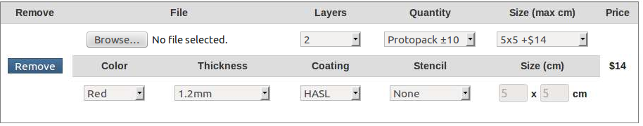
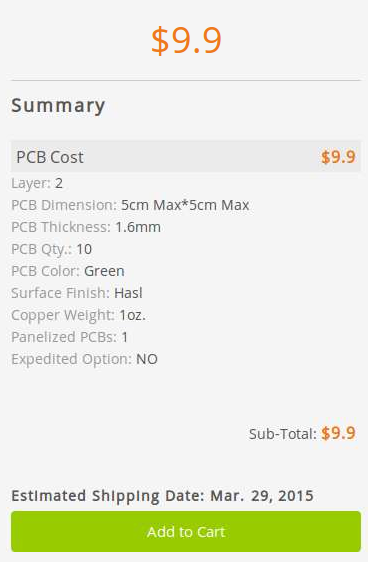
- Select the right most board dimension and drag it until its X coordinate is 50mm. Then drag the top board dimension until its Y coordinate is 50mm. This defines the outer dimensions of the PCB. The choice of 5cmx5cm for the board size is based on the least expensive PCB size that SeeedStudio offers.
 Turn on the following layers “top, pads, vias, unroute, dimension,tPlace,tOrigin,tName,Holes”
 place four 4.3mm holes in the corners of the board at coordinates (3.81,3.175) (45.72,3.175) (45.72,46.355) (3.81, 46.355) To provide fine grain control over the placement use the information tool and select the hole. The information window allows you to enter the exact X,Y position of the hole.
 - Save
Step2 – Placing components
When you first start laying out a PCB all of the schematic components are just dumped to the side of the layout and they need to be moved onto the PCB routing area. We will begin by placing the top side components first and follow that up with the bottom side components.
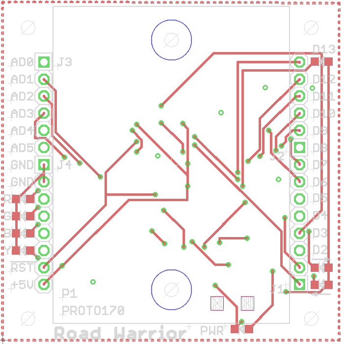
Top (Red layer)
- Turn on the following layers “top, pads, vias, unroute, dimension,tPlace,tOrigin,tName,Holes”
- Move the prototype board to the center of the PCB. It should be located at (25,26)
- Move the connectors onto the board
J1 to (43.942,17.155)
J2 to (43.942,37.473)
J3 to (6.096,32.395)
J4 to (6.096,17.155) - Add text labels to the connector pins Size1.27 ratio 8%
- Move the LEDs onto the PCB
Bottom (Blue Layer)
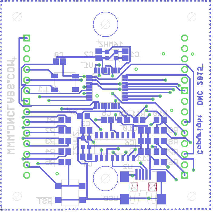
- Turn on the following layers “bottom, pads, vias, unroute, dimension,bPlace,bOrigin,bName,Holes”
 The components are dropped onto the top side of the PCB when the layout was created from the schematic. To place components onto the secondary side of the board they must be mirrored.
 - Move the components onto the board taking care to place them so they don’t overlap. The yellow air wires (unrouted wires) show the logical connections. The goal of the placement is to minimize the length of these air wires.
 The DRC will check for any placement violations. That includes placing components to close to each other or the edge of the board. It is very important that there are no violations at this point.
Step 3 – Routing
To convert the air wires into physical copper traces we will use the autorouter. This is fast but does not result in the most optimal layout. For most Arduino digital designs it will do a good enough job and it is much easier and faster than manually routing a board.
- In the command line type “grid in” to set the dimensions to imperial.
- Turn on the following layers “bottom, pads, vias, unroute, dimension,bPlace,bOrigin,bName,Holes, tPlace,tOrigin,tName “
- Click on the DRC icon and then select the load button. In the panel that opens you can select your routing options. For this project select the default.dru
- Open the Edit menu and scroll to the bottom where it says net classes. You can set the drill and trace widths here. We want to use 20 mils via, 10 mils trace
- Click auto route and set the routing grid to 5mils. Press Ok and wait for the autorouter to complete the job to 100% routed.
- If you are unhappy with the routing you can use “ripup all” in the command line to unroute the board. The ripup only occurs after you click the stop light pattern to accept the change.
- Run the DRC again to check that no additional errors have crept in.
Step 4 – Copper fill
After you are happy with the layout you can optionally apply a copper fill to the PCB. This provides a better ground plane and also helps to keep the board from warping. This should only be applied after you have finished the routing.
 Draw a Polygon around the edge of the PCB. Select the “Layer 1 Top”.
 - Select the Polygon and assign a value of GND to it.
- Repeat for the “Layer 16 Bottom”.
- Press the rats nest and the fill pattern will show up.
Step 6 – Visualize the design with POVRay
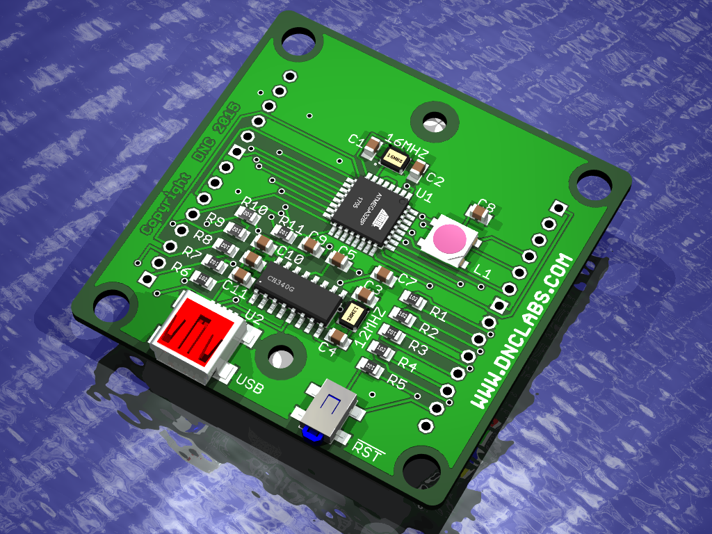
- From the “File” menu select the” Run” ulp icon and then select the 3d41.ulp
- To create a top view of the PCB Select the “Board” tab and set the “Rotation angle board ZYX” to 0,30,0
- Click “Create POV file and exit”
- To create a bottom view of the PCB change the destination file name to “Road_Warriorbot.pov”. Next select the “Board” tab and set the “Rotation angle board ZYX” to 180, 210,0
- Click “Create POV file and exit”
- Go to the windows desktop and find the directory Eagle3DOuput. This directory should exist if you followed the install instructions.
- Click on either the top or bottom POV ray file and it will open in POVRay.
- Click Run in PovRay and your board will be rendered as a 3D photo. The rendered file will be saved in the Eagle3DOuput folder as a *.png file.
Step 7 – Making design files to order boards
- Click “cam processor->Open->Job->Seeed_Gerber_DNC.cam->Open”
- Click “Process Job” and close the cam window
- The cam processor script will generate the Gerber files for your design. The 8 files that are required by the board manufacturer can be found in the Eagle/Project directory. Copy required files to a folder of your choice and zip them
RoadWarrior.GBL
RoadWarrior.GMO
RoadWarrior.GBS
RoadWarrior.GML
RoadWarrior.GTL
RoadWarrior.GTO
RoadWarrior.GTS
RoadWarrior.TXT - Place order with SeeedStudio or DirtyPCB