The goal of this workshop is to capture a schematic design for an Arduino Uno compatible board. The complete schematic will look something like the schematic below. I will provide basic instructions for each step in the process but the majority of the workshop is self directed. I will assist people with any issues that they are having. At the end of the workshop you should be familiar with the basic schematic design tools.
The workshop is deliberately short and I expect that some attendees may not finish their design within the hour. I will attempt to keep us on schedule by introducing each new subject at the times indicated. This will allow us to cover all of the material even if we don’t complete every step. My goal in teaching this workshop is to ensure that everyone leaves with the ability to complete the schematic at home if not during the workshop. When we start the next workshop on routing the PCB I will provide a complete schematic as a starting point.
Step1 – Setting up a new design 5 minutes
- create a project “Road_Warrior”
- create a schematic
- add a frame “A4LOC”
- add text “Road Warrior”, “Copyright your name 2015”
- save as “Road_Warrior”
Step2 – Adding components 10 minutes
Add the following components to the schematic. Place them approximately where I have shown them in the attached schematic. 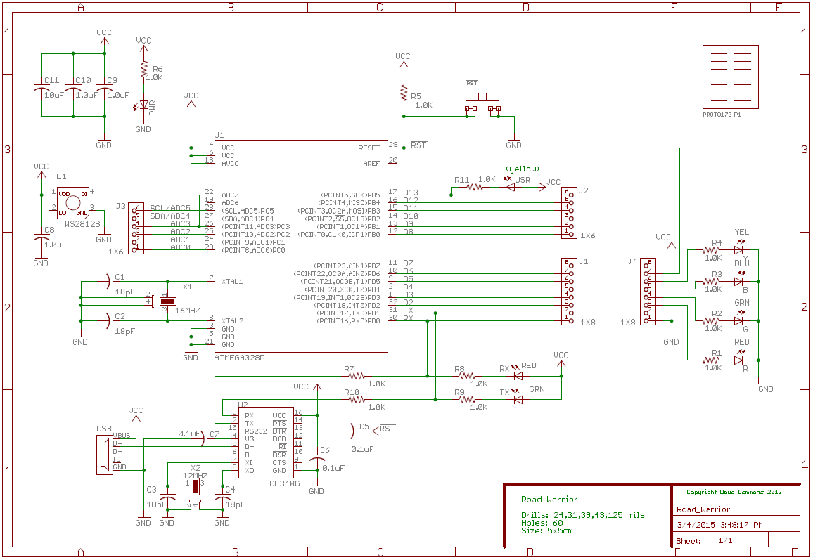 After placing them, they can be moved and turned as required.
Qty Value      Package      Parts
1   PROTO170   PROTO170     P1
2   BLU        LED_0805_BLU B, PWR
2   GRN        LED_0805_GRN G, TX
2   RED        LED_0805_RED R, RX
2   YEL        LED_0805_YEL Y, USR
1   ATMEGA328P TQFP32-08    U1
1   CH340G     SO-16        U2
3   0.1uF      C0805        C5-7
11  1.0K       R0805        R1-11
3   1.0uF      C0805        C8-10
2   1X6        1X6          J2-3
2   1X8        1X8          J1,J4
1   10uF       C0805        C11
1   12MHZ      3.2X2.5_XTAL X2
1   16MHZ      3.2X2.5_XTAL X1
4   18pF       C0805        C1-4
1   USB        USB_CHINA    J5
1   WS2812B    WS2812B      L1
1   SWITCH           	    !RST
![]() move and rotate – Left click the tool icon and then left click the device to be moved. Use the right click to rotate the device.
move and rotate – Left click the tool icon and then left click the device to be moved. Use the right click to rotate the device.
![]() copy – Left click the tool icon and then select the component to copy. Right click to drop copy where you want.
copy – Left click the tool icon and then select the component to copy. Right click to drop copy where you want.
![]() delete – Left click the tool icon and then left click on anything you want to delete.
delete – Left click the tool icon and then left click on anything you want to delete.
![]() group – Left click the icon then click one corner of an area to be grouped. Drag the cursor to select the area and left click again.
group – Left click the icon then click one corner of an area to be grouped. Drag the cursor to select the area and left click again.
Step 3 – Wiring 15 minutes
Using the reference schematic we will wire the circuit connections. After wiring is completed there is a limited error rule check that we can run. The ERC looks for gross errors such as having only one pin on a network. It also looks for components with no values assigned and ambiguous connections. All of these errors should be tidied
![]() wire – Using the wire tool connect the devices together as shown in my sample schematic. You may need to move or rotate components to simplify the wiring. Notice that if you move the component pins so that the pins overlap another component pin they will become connected. Then just drag the component apart to make it tidier. Hint Use this to wire up the 1×6 and 1×8 connectors to save time.
wire – Using the wire tool connect the devices together as shown in my sample schematic. You may need to move or rotate components to simplify the wiring. Notice that if you move the component pins so that the pins overlap another component pin they will become connected. Then just drag the component apart to make it tidier. Hint Use this to wire up the 1×6 and 1×8 connectors to save time.
![]() junction – When two wires connect as a junction it is not clear if they are to be connected so we add a dot symbol to make the connection.
junction – When two wires connect as a junction it is not clear if they are to be connected so we add a dot symbol to make the connection.
value – Left click the tool icon and type a value. Each L,R,C component needs to have a value so go ahead and enter all of the component values.
![]() labels – If you apply a name to a signal net this command will print the net name.
labels – If you apply a name to a signal net this command will print the net name.
![]() ERC – Under the tool menu there is a an error rule check. Click this and it will report any connectivity errors that are uncovered. These all need to be fixed.
ERC – Under the tool menu there is a an error rule check. Click this and it will report any connectivity errors that are uncovered. These all need to be fixed.
Step4 – Making it pretty 30 minutes
At this point we have completed the design but it may not be very easy to read the schematic. Frequently component labels and values cross wiring nets making them unreadable. To tidy the schematic we use the “smash” tool which allows you to move the value and label text independent of the component symbol. This allows you to move and rotate the text for greater readability.
Tip: I like to group select the entire schematic and apply the “smash” all at once.
![]() smash – This tool seperates the name and value from the component symbol so that each is individually moveable. Use this to make the schematic easier to read if the component or name text overlaps a symbol or net.
smash – This tool seperates the name and value from the component symbol so that each is individually moveable. Use this to make the schematic easier to read if the component or name text overlaps a symbol or net.
![]() text – Use text to annotate you design and add details to the caption box in the lower right corner of the schematic.
text – Use text to annotate you design and add details to the caption box in the lower right corner of the schematic.
The other design consideration you may want to consider is the generation of a bill of materials by running the BOM user language program. Eagle assigns component names sequentially in the order which you place them so you may find that you have designed a schematic with 110 ohm resistors labeled R1,R7,R11. I like to re-label the names so that they run sequentially ie) R1-3. Why? This will reduce the board assembly time and help eliminate errors.