 When I designed the capacitive switch I didn’t include any connectors on the board so that it would be as thin as possible. As a result, there is no easy way to program the micro-controller when I first assemble one of the boards. The design of the capacitive sensor board provides 5 solder pads for programming the ATTiny40 processor. Initially I tested my first board by soldering fly wires to the pads and then to a 2×5 IDC connector that plugged into the programmer. I wanted a slightly easier process for programming the cap sense boards; one that didn’t require soldering. The solution I worked out was a laser cut test fixture with pogo pins to contact the board solder pads.
Pogo pins are spring loaded steel pins with a chisel tip. I purchased the pins from Sparkfun. The spring loading ensures that the pin makes good electrical contact with the board pads. The TPI programmer header requires 5 wires so there are five 0.1″ square pads on the PCB which meant I needed to mount the pogo pins in a precise array. When the ATTiny40 board is pressed down into the jig each of the pogo pins contacts one of the PCB pads and allows me to program the board. I first measured the PCB pad positions relative to one corner of the PCB; the measurements were made using the Eagle layout tool which gave me accurate X, Y co-ordinates. Once I had determined the PCB geometry I drew a cutting pattern in Corel Draw. The Corel file could then be printed directly to a 30W Zing Laser which would cut the parts in quarter inch acrylic.
I assembled the acrylic top plates onto a small wooden frame. The frame serves two purposes. First the pogo pins are about 2″ long so I needed clearance under the top plate. Second I needed somewhere to hold the TPI programmer. The pogo pins were epoxied into place so that the brass body was flush with the top of the acrylic which leaves the steel pins extended 1/4″ above the acrylic. Once the glue dried I soldered ribbon cable wire from the pins to the programmer.
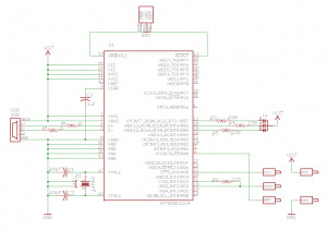
The complete design for the MKII TPI clone is included the Lufa project directory. I have provided a binary file that can be directly loaded onto an ATMega32U4 processor using Flip. The source code is available at http://www.fourwalledcubicle.com/LUFA.php. The schematic shows how I wired the interface pins to the TPI pins of the ATTiny40. Note that the TPI protocol uses the UART in synchronous mode such that the TPI clock is derived from the ATMega32U4 XCLK output pin. This means you can’t arbitrarily move the clock to a different I/O pin unless you decide to bit bang the TPI code.
Results
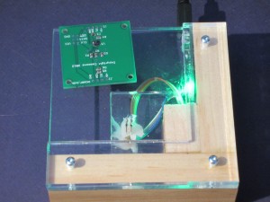
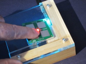
The completed test fixture is shown here programming the capacitive sense switch. The design works well and certainly speeds up the task of programming the new boards. However, after building the test jig I have found a number of issues that I want to fix.
The pogo pins are too long so that the board that is being programmed does not lie flat in the test fixture.
The long pin tails required additional mechanical support to keep the pins straight. I kludged a second support here.
Hand soldering the wires from the programmer board to the pogo pins seems a little fragile.
TPI binary: AVRISP-MKII-TPI.hex